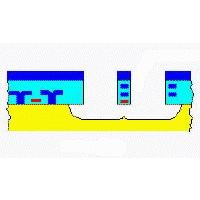
High-Aspect-Ratio CMOS Micromachining Process

This Project is no longer active.
Carnegie Mellon has developed an integrated CMOS- MEMS process in which electrostatically actuated microstructures with high-aspect-ratio (about 5:1) composite-beam suspensions are fabricated using conventional CMOS processing followed by a sequence of maskless dry-etching steps. The key feature of the technology is the ability to make composite metal/insulator microstructures with very narrow beam widths and air gaps, enabling lateral motion and electrostatic actuation with a wide range of electromechanical sensor and actuator design possibilities. The CMOS metallization and dielectric layers, normally used for electrical interconnect, now serve a dual function as a structural layer. Another important point is that no standard CMOS design rules are broken in the layout of the CMOS-MEMS devices, thereby ensuring working devices and compatibility with most CMOS processes.
